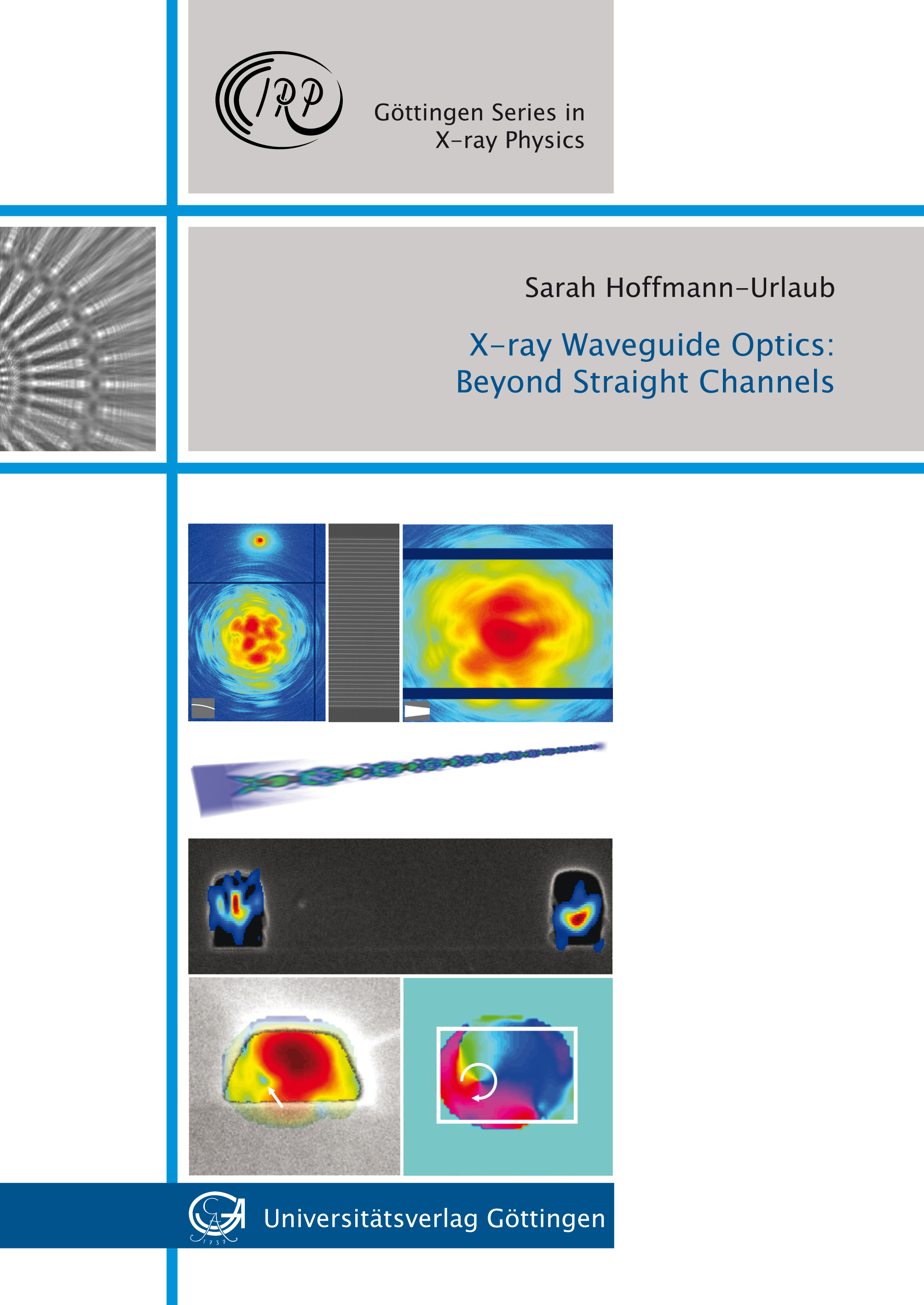
Modern x-ray sources and analysis techniques such as lens less imaging combined with phase retrieval algorithms allow for resolving structure sizes in the nanometer range. For this purpose optics have to be employed, ensuring small focal spot dimensions simultaneously with high photon densities. Furthermore, the wave front behind the optics is required to be smooth enabling for high resolution imaging. Combining all these properties, x-ray waveguides are well suited to perform this task, since the intensity distribution behind the guide is restricted in two dimensions serving as a secondary quasi point-source without wave-front aberrations, showing also a high divergence, suitable for resolving fine features. Importantly, the radiation provided by the waveguide reveals a high degree of coherence, required by many imaging techniques. The waveguide itself consists of an air-filled channel embedded in a solid matrix; typical materials are silicon, germanium or quartz. While the entrance area is nano-sized, the channel length is in the millimeter-range, this way posing challenges to fabricate high aspect ratio geometries. Since the functioning of x-ray waveguides is based on the total reflection at small incident angles, the surface roughness of the channel walls must be as low as possible to avoid scattering and hence loss of intensity. To fulfill these demanding conditions, a process scheme involving spin-coating, electron beam lithography, wet development, reactive ion etching and wafer bonding is optimized within this work. To gain deeper insights into the principle of wave guiding finite difference simulations are performed, also opening access for advanced design considerations such as gratings, tapered and curved channels, or beamsplitters, enabling for constructing novel x-ray tools as for example time delay devices or interferometers. Waveguides in all geometries are tested at synchrotron sources, accomplishing new benchmarks in x-ray optical performance. Here, the x-ray beam leaving the channel, propagates out to a pixel array detector in the far-field region. From the recorded data the intensity distribution in the near-field directly behind the waveguide is reconstructed, revealing an outstanding agreement with the simulations and electron micrographs. Since the radiation field of the waveguide is well-characterized and also tunable to meet the requirements of both the measurement setup and the sample, they are suited of a broad field of applications in coherent x-ray imaging.
Publikationstyp: Hochschulschrift
Sparte: Universitätsverlag
Sprache: Englisch


